- 您现在的位置:买卖IC网 > Sheet目录3871 > PIC18F1230T-I/SO (Microchip Technology)IC PIC MCU FLASH 2KX16 18SOIC
PIC18F1230/1330
DS39758D-page 160
2009 Microchip Technology Inc.
15.2.2
EUSART ASYNCHRONOUS
RECEIVER
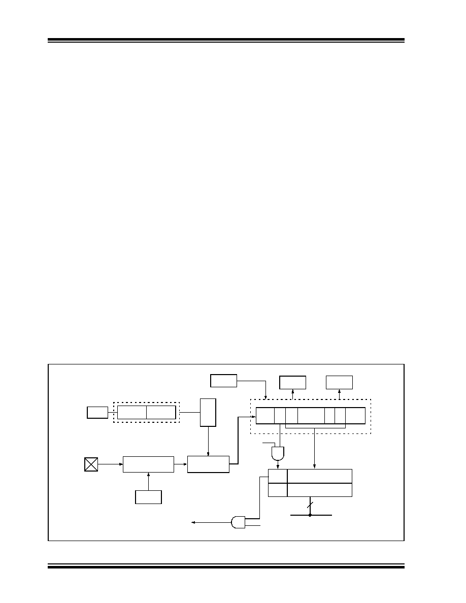
The receiver block diagram is shown in Figure 15-6.
The data is received on the RX pin and drives the data
recovery block. The data recovery block is actually a
high-speed shifter operating at x16 times the baud rate,
whereas the main receive serial shifter operates at the
bit rate or at FOSC. This mode would typically be used
in RS-232 systems.
To set up an Asynchronous Reception:
1.
Initialize the SPBRGH:SPBRG registers for the
appropriate baud rate. Set or clear the BRGH
and BRG16 bits, as required, to achieve the
desired baud rate.
2.
Enable the asynchronous serial port by clearing
bit SYNC and setting bit SPEN.
3.
If interrupts are desired, set enable bit RCIE.
4.
If 9-bit reception is desired, set bit RX9.
5.
Enable the reception by setting bit CREN.
6.
Flag bit, RCIF, will be set when reception is
complete and an interrupt will be generated if
enable bit, RCIE, was set.
7.
Read the RCSTA register to get the 9th bit (if
enabled) and determine if any error occurred
during reception.
8.
Read the 8-bit received data by reading the
RCREG register.
9.
If any error occurred, clear the error by clearing
enable bit CREN.
10. If using interrupts, ensure that the GIE and PEIE
bits in the INTCON register (INTCON<7:6>) are
set.
15.2.3
SETTING UP 9-BIT MODE WITH
ADDRESS DETECT
This mode would typically be used in RS-485 systems.
To set up an Asynchronous Reception with Address
Detect Enable:
1.
Initialize the SPBRGH:SPBRG registers for the
appropriate baud rate. Set or clear the BRGH
and BRG16 bits, as required, to achieve the
desired baud rate.
2.
Enable the asynchronous serial port by clearing
the SYNC bit and setting the SPEN bit.
3.
If interrupts are required, set the RCEN bit and
select the desired priority level with the RCIP bit.
4.
Set the RX9 bit to enable 9-bit reception.
5.
Set the ADDEN bit to enable address detect.
6.
Enable reception by setting the CREN bit.
7.
The RCIF bit will be set when reception is
complete. The interrupt will be Acknowledged if
the RCIE and GIE bits are set.
8.
Read the RCSTA register to determine if any
error occurred during reception, as well as read
bit 9 of data (if applicable).
9.
Read RCREG to determine if the device is being
addressed.
10. If any error occurred, clear the CREN bit.
11. If the device has been addressed, clear the
ADDEN bit to allow all received data into the
receive buffer and interrupt the CPU.
FIGURE 15-6:
EUSART RECEIVE BLOCK DIAGRAM
x64 Baud Rate CLK
Baud Rate Generator
RX
Pin Buffer
and Control
SPEN
Data
Recovery
CREN
OERR
FERR
RSR Register
MSb
LSb
RX9D
RCREG Register
FIFO
Interrupt
RCIF
RCIE
Data Bus
8
64
16
or
Stop
Start
(8)
7
1
0
RX9
SPBRG
SPBRGH
BRG16
or
4
发布紧急采购,3分钟左右您将得到回复。
相关PDF资料
PIC18F1330T-I/ML
IC PIC MCU FLASH 4KX16 28QFN
PIC18F65J50T-I/PT
IC PIC MCU FLASH 16KX16 64TQFP
PIC18F83J11T-I/PT
IC PIC MCU FLASH 4KX16 80TQFP
PIC16LF627-04/P
IC MCU FLASH 1KX14 COMP 18DIP
PIC18F86J55T-I/PT
IC PIC MCU FLASH 48KX16 80TQFP
PIC18F43K22-I/MV
MCU PIC 8KB FLASH 40QFN
PIC16C55A-04I/P
IC MCU OTP 512X12 28DIP
PIC18LF43K22-I/MV
MCU PIC 8KB FLASH 40UQFN
相关代理商/技术参数
PIC18F1230T-I/SS
功能描述:8位微控制器 -MCU 4KB Flash 256 RAM RoHS:否 制造商:Silicon Labs 核心:8051 处理器系列:C8051F39x 数据总线宽度:8 bit 最大时钟频率:50 MHz 程序存储器大小:16 KB 数据 RAM 大小:1 KB 片上 ADC:Yes 工作电源电压:1.8 V to 3.6 V 工作温度范围:- 40 C to + 105 C 封装 / 箱体:QFN-20 安装风格:SMD/SMT
PIC18F1320-E/ML
功能描述:8位微控制器 -MCU 8KB 256 RAM 16 I/O RoHS:否 制造商:Silicon Labs 核心:8051 处理器系列:C8051F39x 数据总线宽度:8 bit 最大时钟频率:50 MHz 程序存储器大小:16 KB 数据 RAM 大小:1 KB 片上 ADC:Yes 工作电源电压:1.8 V to 3.6 V 工作温度范围:- 40 C to + 105 C 封装 / 箱体:QFN-20 安装风格:SMD/SMT
PIC18F1320-E/P
功能描述:8位微控制器 -MCU 8KB 256 RAM 16 I/O RoHS:否 制造商:Silicon Labs 核心:8051 处理器系列:C8051F39x 数据总线宽度:8 bit 最大时钟频率:50 MHz 程序存储器大小:16 KB 数据 RAM 大小:1 KB 片上 ADC:Yes 工作电源电压:1.8 V to 3.6 V 工作温度范围:- 40 C to + 105 C 封装 / 箱体:QFN-20 安装风格:SMD/SMT
PIC18F1320-E/SO
功能描述:8位微控制器 -MCU 8KB 256 RAM 16 I/O RoHS:否 制造商:Silicon Labs 核心:8051 处理器系列:C8051F39x 数据总线宽度:8 bit 最大时钟频率:50 MHz 程序存储器大小:16 KB 数据 RAM 大小:1 KB 片上 ADC:Yes 工作电源电压:1.8 V to 3.6 V 工作温度范围:- 40 C to + 105 C 封装 / 箱体:QFN-20 安装风格:SMD/SMT
PIC18F1320-E/SS
功能描述:8位微控制器 -MCU 8KB 256 RAM 16 I/O RoHS:否 制造商:Silicon Labs 核心:8051 处理器系列:C8051F39x 数据总线宽度:8 bit 最大时钟频率:50 MHz 程序存储器大小:16 KB 数据 RAM 大小:1 KB 片上 ADC:Yes 工作电源电压:1.8 V to 3.6 V 工作温度范围:- 40 C to + 105 C 封装 / 箱体:QFN-20 安装风格:SMD/SMT
PIC18F1320-H/ML
功能描述:8位微控制器 -MCU 8KB FL 256RAM 16 I/O RoHS:否 制造商:Silicon Labs 核心:8051 处理器系列:C8051F39x 数据总线宽度:8 bit 最大时钟频率:50 MHz 程序存储器大小:16 KB 数据 RAM 大小:1 KB 片上 ADC:Yes 工作电源电压:1.8 V to 3.6 V 工作温度范围:- 40 C to + 105 C 封装 / 箱体:QFN-20 安装风格:SMD/SMT
PIC18F1320-H/P
功能描述:8位微控制器 -MCU 8KB FL 256RAM 16 I/O RoHS:否 制造商:Silicon Labs 核心:8051 处理器系列:C8051F39x 数据总线宽度:8 bit 最大时钟频率:50 MHz 程序存储器大小:16 KB 数据 RAM 大小:1 KB 片上 ADC:Yes 工作电源电压:1.8 V to 3.6 V 工作温度范围:- 40 C to + 105 C 封装 / 箱体:QFN-20 安装风格:SMD/SMT
PIC18F1320-H/SO
功能描述:8位微控制器 -MCU 8KB FL 256RAM 16 I/O RoHS:否 制造商:Silicon Labs 核心:8051 处理器系列:C8051F39x 数据总线宽度:8 bit 最大时钟频率:50 MHz 程序存储器大小:16 KB 数据 RAM 大小:1 KB 片上 ADC:Yes 工作电源电压:1.8 V to 3.6 V 工作温度范围:- 40 C to + 105 C 封装 / 箱体:QFN-20 安装风格:SMD/SMT